PCB
Departmental facilities to manufacture PCBs

- Flat bed CNC milling
- Chemical Etching
- Laser ablation
Holes, slots and edges are cut using ether a cnc milling machine or laser ablation
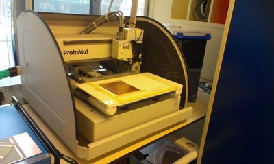
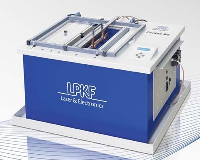
In the department there are 2 CNC milling machines, a spray etch tank and laser ablation system to produce PCBs. The etching and CNC milling machines are in the EE workshop (T-Tech Quick Circuit 7000, LPKF - Protomat S103 and mega Roto - Spray).

The machines have different design constraints thus we can cater for most types of PCB (Analogue, Digital, Antennas, Wave guides, Micro Strips, mixed signal, etc); Below gives you the information required for us to manufacture your board.
PCB Specifications
Minimum & Maximum Dimensions
| Material Size (Bed Size) | T-tech milling : 430mm x 300mm | S103 milling : 220mm x 300mm | Chemical Etch : 220mm x 300mm | Laser ablation : 220mm x 300mm |
|---|---|
| Board Thickness | T-Tech milling : 0.5mm to 2.5mm | S103 milling : 0.5 to 3mm | Chemical Etch : Any | Laser ablation : 0.2 to 7mm |
| Minimum separation between tracks and pads |
T-Tech milling : 0.28mm (NOTE: we can go smaller but the cut my not be uniform) S103 milling : 0.25mm (NOTE: we can go smaller but the cut my not be uniform) Chemical Etch : 0.3mm (smaller can be done if professional masks are produced from an external supplier) Laser ablation : 30um |
| Minimum track width |
T-Tech milling : 0.25mm ( NOTE: Varies depending on material, we can go smaller but there is a risk of losing a pad / track ) S103 milling : 0.25mm ( NOTE: Varies depending on material, we can go smaller but there is a risk of losing a pad / track ) Chemical Etch : 0.3mm ( NOTE: Varies depending on size of pcb, material and quality of etch resist ) Laser ablation : 0.1mm ( NOTE : Can go smaller but depends on material ) |
| NOTE |
All board material must have at least a minimum of 2cm clearance between the edge of your material and your design. This is for positioning, fiducial alignment and if THP plated is required a 3cm clearance must be used for clamping to electrodes. |
Drill Holes
Milling and Chemical Etching
Drill Hole Sizes
0.023"(0.6mm), 0.031”(~0.8mm), 0.036”(~0.9mm), 0.394"(1mm), 0.0512"(~1.3mm), 0.0630”(~1.6mm), 0.0787”(~2mm), 0.125”(~3.1mm)
Holes above and between drill sizes over 0.8mm can be routed to size rather than drilled but can leave a rougher cut.
Laser ablation
Drill Hole size
0.1mm and greater. NOTE : minimum hole size varies with board thickness
The Design
We software we recommend is Diptrace. Other packages can be used but see Andy, Martin or Gerald first. DO NOT USE EAGLE CAD OR CST due to poor exports of CAM \ Gerber \ Drill files.
Eagle designs can be imported into DipTrace but some errors can persist, CST designs can be imported as DXF but errors can persist. We only accept EAGLE and CST as last resort options as it can be very time consuming converting data types, thus resulting in slow manufacture and in some cases poor quality boards.
Make sure that the minimum and maximum rules above have not been broken or there could be complications when making the board.
Designs produced with DipTrace can be sent as is. Other applications you will need to convert the pcb design into a Gerber format for copper tracks, board edge and NC-Drill Excellon format for drill holes.
A Gerber format produces a number of different files depending on the layers used in the design. (sometimes an aperture file is required depending on package and Gerber Format).
For Best results use a minimum of 5 layers e.g. Top Side, Bottom Side, Edge, Top Silk Screen and Bottom Silk Screen.
The NC-Drill / Excellon Format, This produces 2 or more drill files supplying the tool data in one file and hole placement data in the other.
All pcb designs and files must sent via email to pcb-jobs@ee.ucl.ac.uk and it is recommend to submit a 1:1 print out of the circuit showing drill hole sizes encase of import and conversion problems.
Material

Basic PCB material can be purchased from Farnell, RS, HoldersTechnology and MegaUK. if your design is high frequency I would recommend Rogers RT/duroid (www.rogers-corp.com) which is a very good supplier of material.
All PCB Material used must NOT be layered with photo resist, if your board comes with it make sure you remove the resist first.
The we keep a small stock of FR4 ( Data Sheet ) Single sided and Double sided, you can use this board for your project depending if it will fit your design, if not you will have to purchase some.
The materail shoud be large enough to fit your design with some over hang see image below
Things To Avoid

This design contains some of the common problems we have encountered during PCB manufacture:-
(1) The vias are smaller than the standard drill hole, if we attempt to drill out these holes the drill would remove the copper pad making it imposable to solder the via.
(2) These tracks are too thin (size 0.01”), these are at risk of lifting or being removed/damaged in the milling process.
If you have thin track consult us before you give us the finished design.
(3) Try to avoid running tracks between pads of a chip, the track must be very thin to do so which means the track has the same problem as in (2).
(4) Edge Connectors Make sure the connector is seated in the correct position and firmly in place, as the solder connections can be placed under stress once a cable is connected. If the socket is to be panel mounted make sure that it over hangs the board.
(*5) Try to avoid connecting a track to an IC on the topside. This can make soldering harder and you can end up melting the chip holder. Instead bring out a track on the bottom side and use a via to take the track to the topside.
(6) Try to avoid placing pads close to tracks, in this case the gap between the pad and track is less that 11 thou (0.28mm) so we would not be able to remove the copper in this area.
(*7) Try to avoid placing tracks to the topside of a connector, in some cases the edge connector may cover the pads stopping you from soldering the pins. Check the connector diagram to see which pins can be soldered to on which side of the board
(NOTE: 5 and 7 can be used if through hole plating but it is still risky if a few holes fail to plate fully)
Layer list:
| Blue | Top side |
|---|---|
| Red | Bottom side |
| Yellow | Board edge and Silk |
| White | Both sides |
Through Hole Plating

In your design we would recommend adding an extra 0.1mm to the hole diameter if plating is required i.e. 0.8mm hole would become 0.7mm after plating so if 0.8mm is required a minimum hole of 0.9mm should be used.
Pads should be a minimum of 0.6mm larger than the hole (so a 1mm hole = 1.6mm pad), the larger the pad the better.
Designs can not use a full panel when plating as the material needs clamping and plating is only even in the center of the board.
PCB Software
In the lab we have the full version of DipTrace installed to design your circuit boards.
Dip trace Full Version
This is a very good easy to use package which is unlimited, which can be used to design your schematics and PCB layouts.
it has libraries containing all the components used in the laboratory and more including SMT components. It can be used to make any type of circuit from though hole to surface mount and multi-layer boards.
The program is extremely easy to use and is the most popular among students for final year projects. The software allows quick and easy board design and export functions to transfer design pictures into other packages such as MS word, also it is capable of importing from other packages such as AutoCad and eagle.
A Freeware 300pin version can be downloaded from DipTrace for students to use on there own computers.